Research and Development Activities
研究開発体制
Our company is actively engaged in research and development activities aimed at reducing costs and ultimately realizing a global de facto standard, with the theme of "developing an environmentally friendly, low-cost construction method." Our research and development activities can be broadly divided into
- Development of new products and technologies that meet current market demands
- Development of new technologies for printed circuit boards that are expected to be realized in the near future or within the next few years, and new technologies for practical application
- Printed circuit board element technology, next-generation boards, special boards
In addition, it also involves developing the most appropriate technologies for mass production, quality and reliability improvement, energy saving, environmental technology, etc. at each production base and deploying them to all bases.
These specific development themes are introduced below.
M-VIA Embedded®
We are working on technologies for embedding narrow-pitch electrode bare chips and small passive components to further increase the performance and miniaturization of mobile devices.In addition, as the need for embedding power ICs in automobiles has increased in recent years, we are actively working on technologies for embedding components and simulation technologies that achieve high current and high heat dissipation.
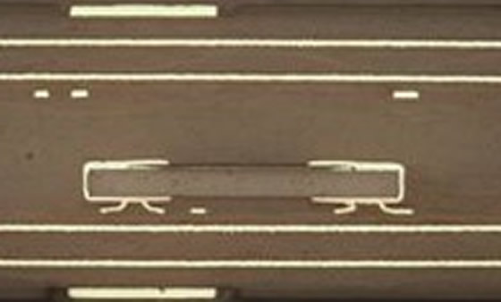
Ultra-Heavy Copper PCBs
We are working on developing ultra-thick copper boards that can carry large currents by increasing the copper thickness of the wiring layer and creating a multi-layer structure.We are working on increasing the thickness of the wiring layer and integral molding using the same resin, and are developing board formation technology that can handle large currents and is highly reliable.
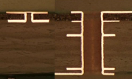
High-frequency hybrid substrate
By creating a hybrid structure using a variety of high-frequency materials (PTFE, LCP, PPE, Low-k Epoxy) and general materials (FR-4), we are able to integrate high-frequency circuits and control circuits to make thinner and smaller boards.We are also working on forming microvias and multi-layering high-frequency materials for higher density wiring.We also conduct in-house evaluations of the material properties and transmission characteristics of new high-frequency materials.
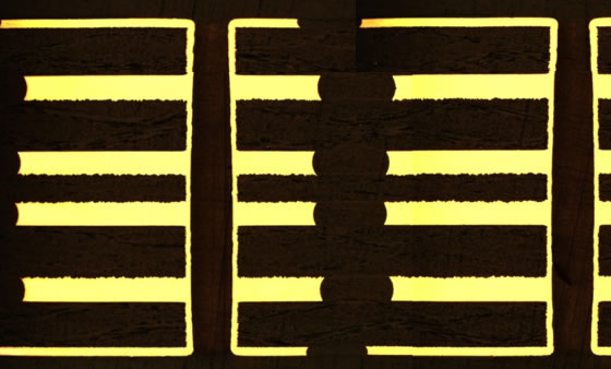
0.3mm Patch CSP Mounting Substrate (M-VIA Any™)
As mobile devices such as smartphones become smaller, lighter, and more multifunctional, 0.35mm pitch CSPs and 0.3mm pitch CSPs are expected to become mainstream in the future. We are working to develop full-layer build-up structures, smaller laser via diameters, smaller via lands, and narrow-pitch circuit formation technologies to accommodate these wiring needs.
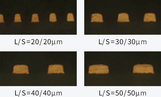
Semi-additive HDI PCBs
To achieve even finer pitch and higher pin count CSPs, it is necessary to increase the number of wires between CSP electrodes from the current 1 to 2 or more, thereby increasing wiring capacity. This will require fine wiring formation technology with L/S = 40/40 μm or less, so we are working on developing a copper foil-based semi-additive method to replace the conventional etching method.