


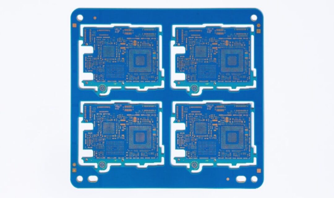
HDI PCBs
HDI PCBss are multilayer boards in which conductor patterns are created on insulating layers, and then layers are stacked one by one using laser technology, plating technology, etc. They allow for higher density and integration than typical multilayer through-hole boards, and are used in devices that require high-density wiring in a limited space. At MEIKO Labo, we manufacture HDI PCBss from 4 to 10 layers, and now you can order products with general specifications online, starting with our easy-quote Standard. Please feel free to use our services for small orders for development and prototyping purposes.
HDI PCBs features
- Many domestic and international manufacturers have adopted our products for automotive and consumer electronics.
- High quality, high durability
- High-density wiring possible
Main uses
-

Automotive navigation system
-

Automotive
-

Wearable devices
-

Digital camera
Contact About the productInquiry
In addition to major corporate clients, we also serve universities, research institutes,
We also accept consultations from venture companies.
We also accept one-off orders from design companies and parts trading companies,
Please feel free to contact us for technical advice.

