


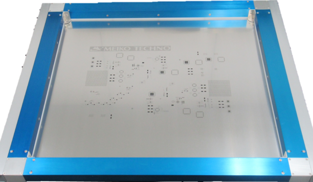
Printed
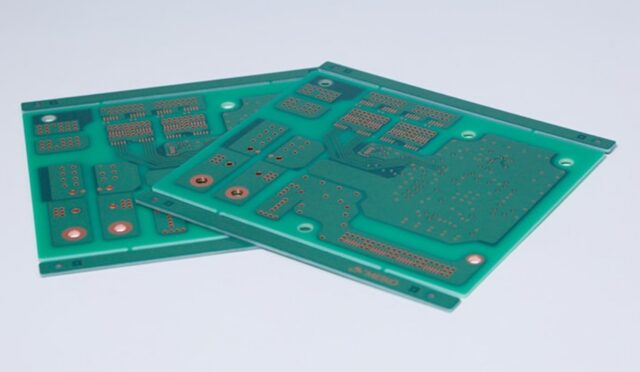
Circuit Board
Printed circuit board design and manufacturing
Circuit Board

Top
Printed circuit board design and manufacturing
How to search
Categories
Categories
Categories
-
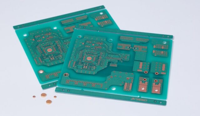
Copper Inlay PCBs
substrate -
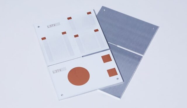
Metal Base Heat DIssipation PCBs
substrate -
Mega Thru Hole
substrate -
Liquidloop Heat Dissipation
substrate -
Millimeter Wave Radar PCBs
substrate -
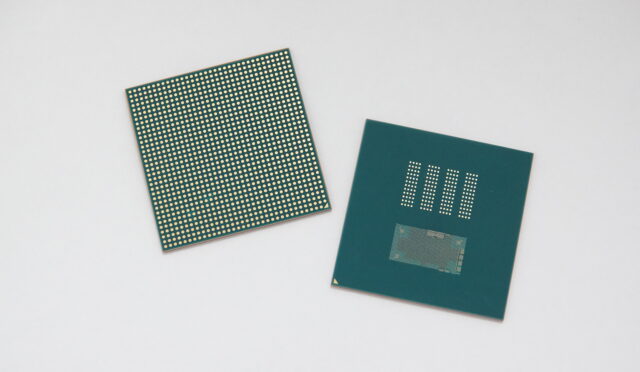
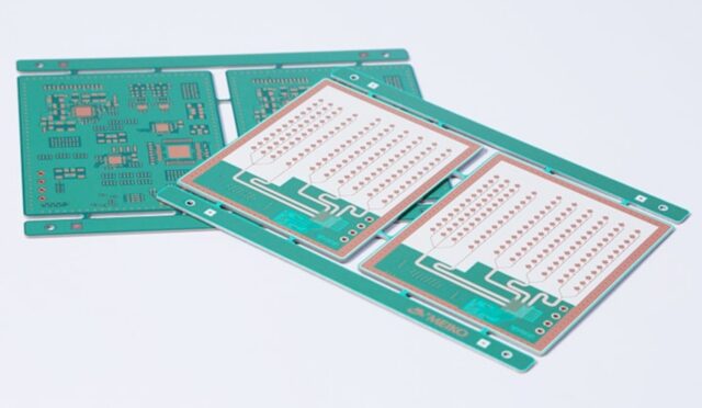
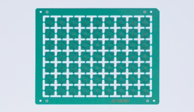
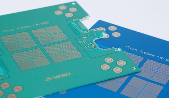
Semiconductor Package Substrate
substrate -
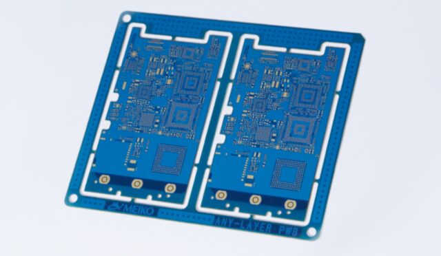
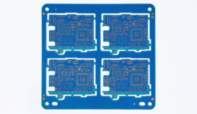
Any Layer PCBs
substrate -
Embedded Device PCBs
substrate -
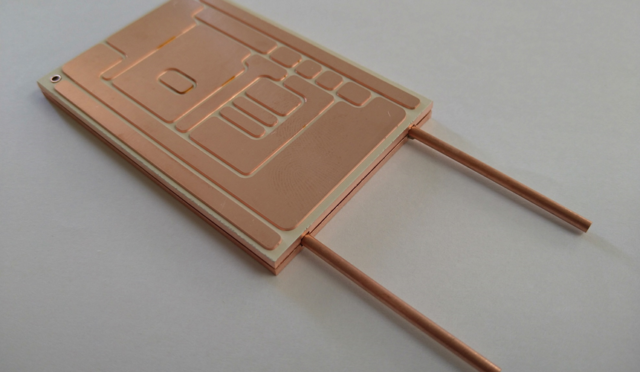
Heavy Copper PCBs
substrate -
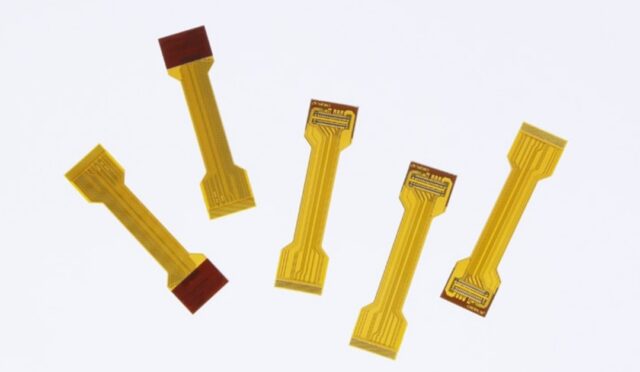
FPC (flexible printed circuit board)
substrate -
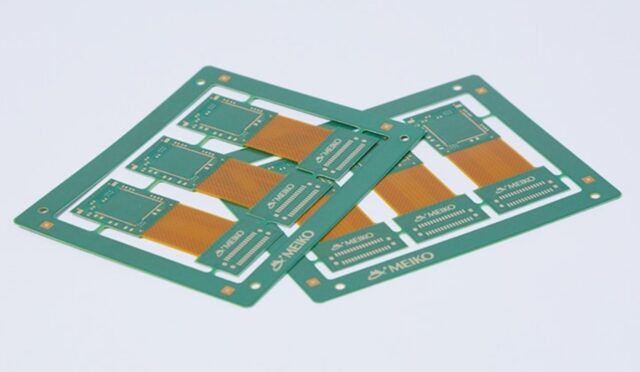
Rigid-Flex PCBs
substrate -
FR4-FLEX/M-VIA Flex®
substrate -
Through-hole PCB
substrate -
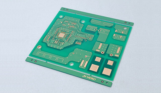
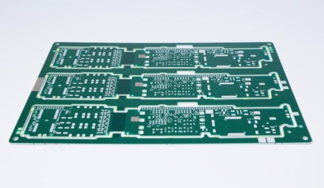
HDI PCBs
substrate -
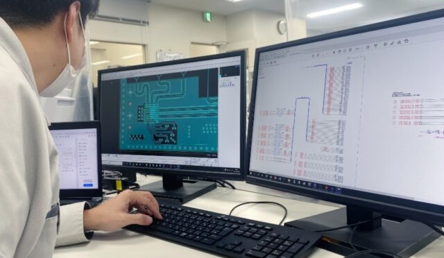
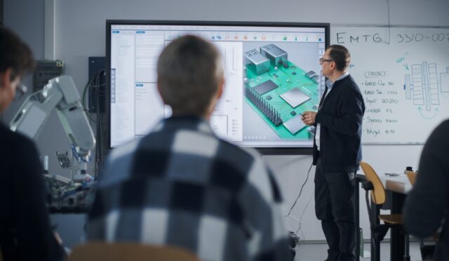
Various designs (structural design, circuit design, AW design)
service -
Mounting jig
service -
Metal mask
service -
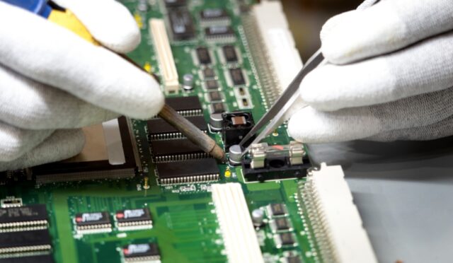
Component Mounting
service -
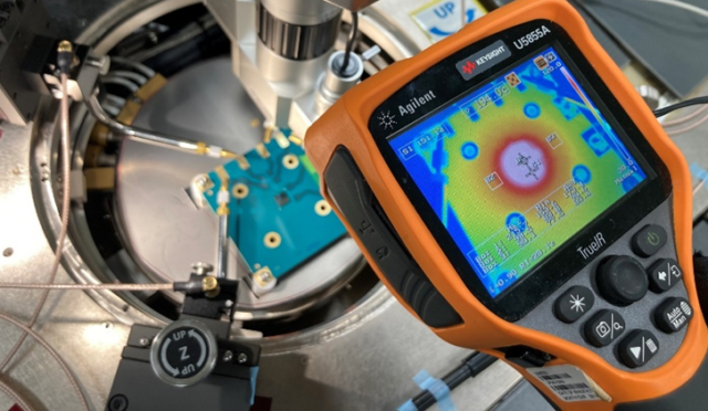
Measurement substrate manufacturing/characteristic evaluation
service -
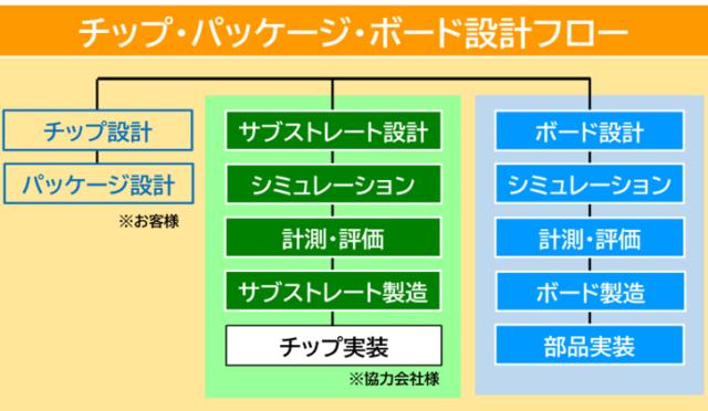
Package and board level co-design verification
service -
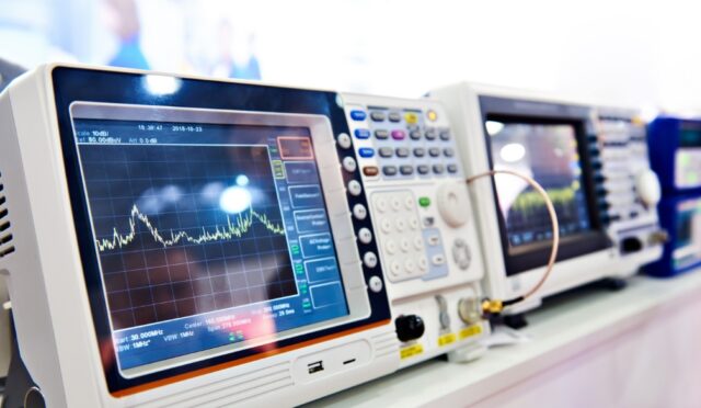
High frequency measurement/simulation
service -
One-stop service
service - There is no information that matches the keyword.