


Package and board level co-design verification
With the technology we have cultivated through the manufacturing, mounting and evaluation of printed wiring boards,
We support our customers in principle verification and advanced development.
Measurement of material dielectric properties and transmission line properties up to 100GHz band,
We provide electromagnetic field analysis, thermal analysis, stress analysis, and measurement board manufacturing.
Top
Development and manufacturing of various mechatronics products
Package and board level co-design verification
01
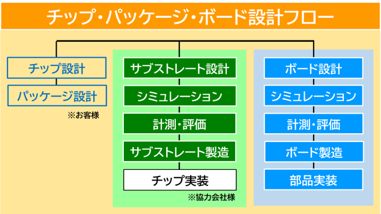
Overall picture of package-board level co-design verification
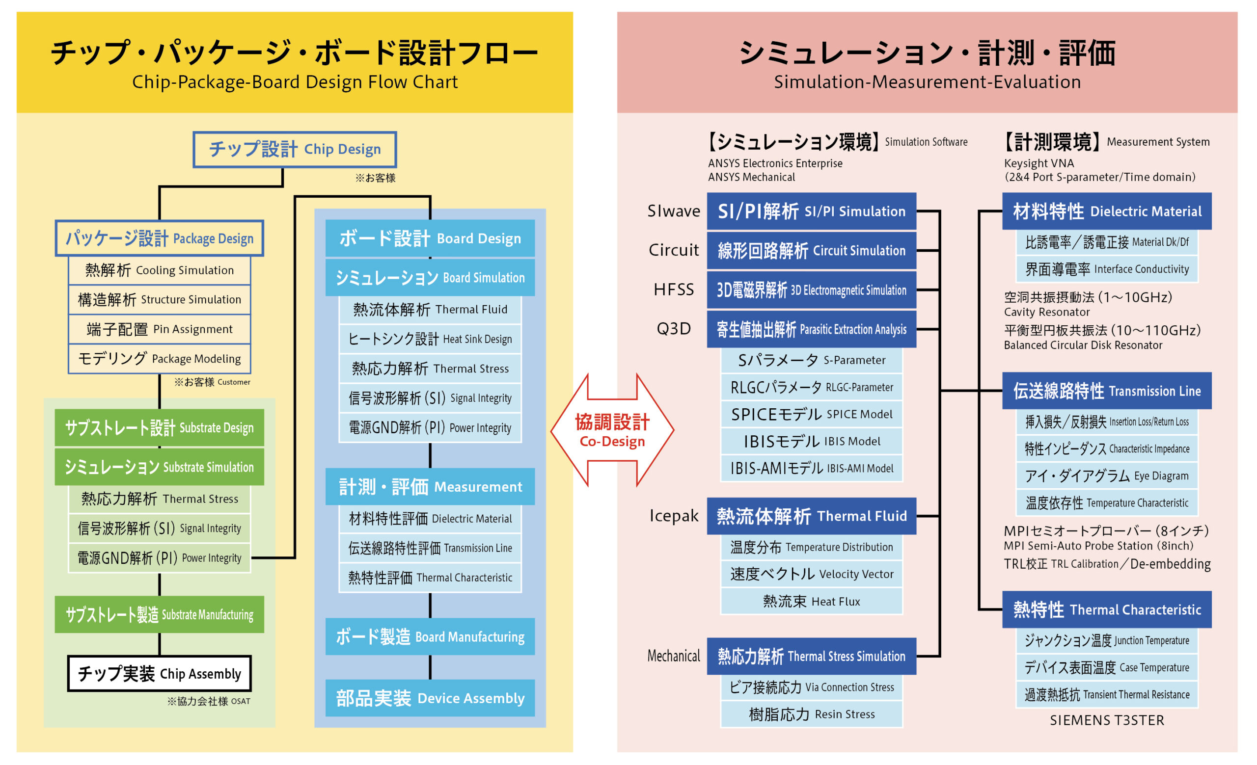
The customer designs the chip and package, and Meiko handles everything from substrate design to board component mounting.
We also support our customers' development by conducting SI/PI analysis, thermal analysis, stress analysis, material dielectric property measurement, transmission line property measurement, and thermal property measurement.
We also support our customers' development by conducting SI/PI analysis, thermal analysis, stress analysis, material dielectric property measurement, transmission line property measurement, and thermal property measurement.
02
Orders received
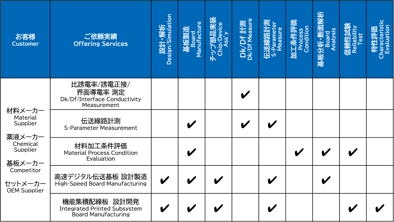
We have provided package and board level collaborative design services to material manufacturers, chemical liquid manufacturers, circuit board manufacturers, and set manufacturers.
We respond to a wide range of inquiries from customers in a wide range of fields.
We respond to a wide range of inquiries from customers in a wide range of fields.
03
Material dielectric properties Measurement environment
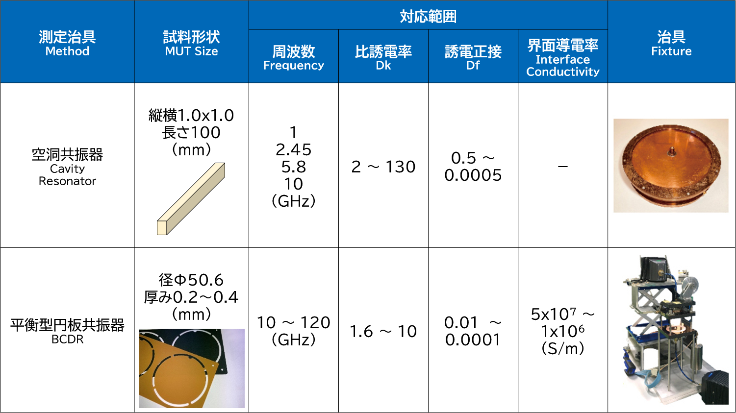
Measures dielectric constant, dielectric loss tangent, and interfacial conductivity up to the millimeter-wave frequency band.
・1GHz~10GHz : Cavity resonator
・10GHz~120GHz : Balanced disc resonator
・1GHz~10GHz : Cavity resonator
・10GHz~120GHz : Balanced disc resonator
04
Transmission line characteristics Measurement environment
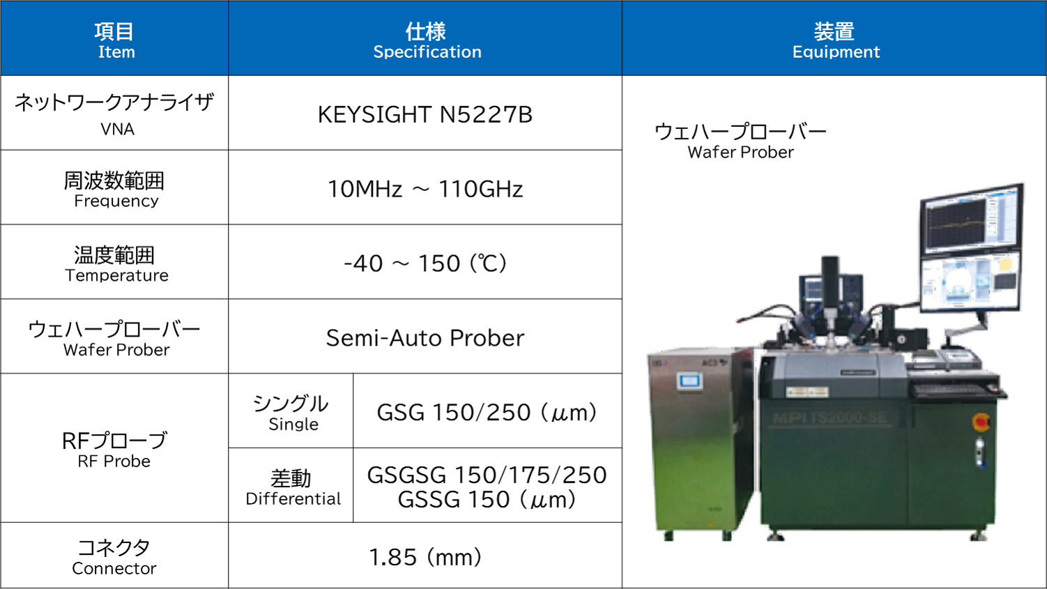
Measures transmission line S-parameters up to the millimeter-wave frequency band.
・Measurement using an RF probe
・Measurement using RF connector
・High-precision positioning using a wafer prober
・Eye diagram measurement
・Measurement using an RF probe
・Measurement using RF connector
・High-precision positioning using a wafer prober
・Eye diagram measurement
Contact About the productInquiry
In addition to major corporate clients, we also serve universities, research institutes,
We also accept consultations from venture companies.
We also accept one-off orders from design companies and parts trading companies,
Please feel free to contact us for technical advice.

