PRODUCT
- HOME
- Products
Meiko provides a wide range of services,
including design and manufacturing of printed circuit boards,
component mounting and assembly,
development of various mechatronics and solution services.
-
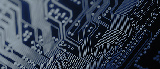
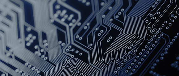
Printed Circuit Board Design and Manufacturing
We provide various cutting-edge products such as high-density and high-frequency, high heat dissipation and large current, and flexibility.
-
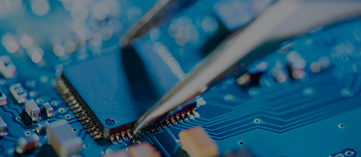
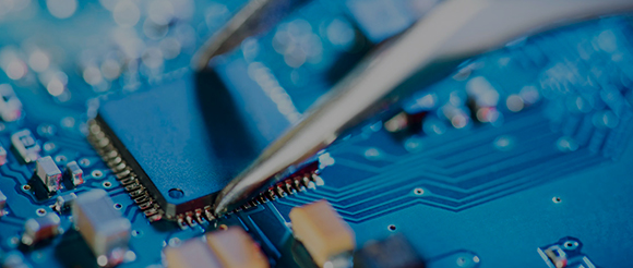
EMSMounting and Assembly
We provide total solutions that can unify the outsourcing of integrated processes from design, PCB manufacturing, mounting, assembly, and shipping.
-
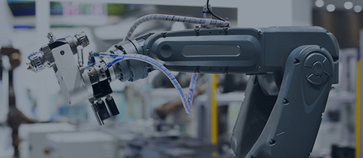
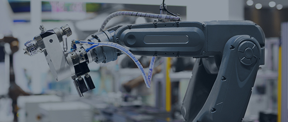
Mechatronic Products Development and Manufacturing
We develop and manufacture equipment and software that solves problems and defects that occur in the field with high technology.
-


Video related EquipmentDevelopment and Manufacturing
The "multi-vision system" developed by Meiko has a great effect on grasping various information.
Find our products by application


Automotive


Telecommunications


Industrial equipment
Medical equipment


Amusement