About
Our Business
Business
01
Printed circuit board business
Circuit Design
We have the latest CAD systems in place to quickly design the best wiring in a limited space. By incorporating Meiko's manufacturing know-how from the design stage, we can ensure a smooth transition to mass production.
Metal mask
Backed by a wide range of experience from design to mounting for mobile devices, automobiles, consumer devices, and more, Meiko provides highly reliable, highly accurate, and high-quality metal masks using cutting-edge equipment.
Furthermore, our integrated production system for manufacturing and sales allows us to achieve the shortest delivery times in the industry.
Furthermore, our integrated production system for manufacturing and sales allows us to achieve the shortest delivery times in the industry.
Mounting jig equipment
We offer mounting jigs and equipment such as board jigs and resin processing, taking advantage of the strengths unique to a board manufacturer.
We will propose the most suitable mounting products and services based on our many years of experience and knowledge.
We will propose the most suitable mounting products and services based on our many years of experience and knowledge.
02
Electronic equipment business
Industrial Equipment
We provide solutions related to automation equipment, such as soldering robots that automate and reduce labor required for post-soldering in the board mounting process, and material handling devices for each manufacturing process.
Video equipment
Our imaging division develops and manufactures the world's first image enlargement device (processor) for multi-vision systems, as well as peripheral devices such as matrix switchers and converters, which are widely used both domestically and overseas.
03
Research and Development Activities
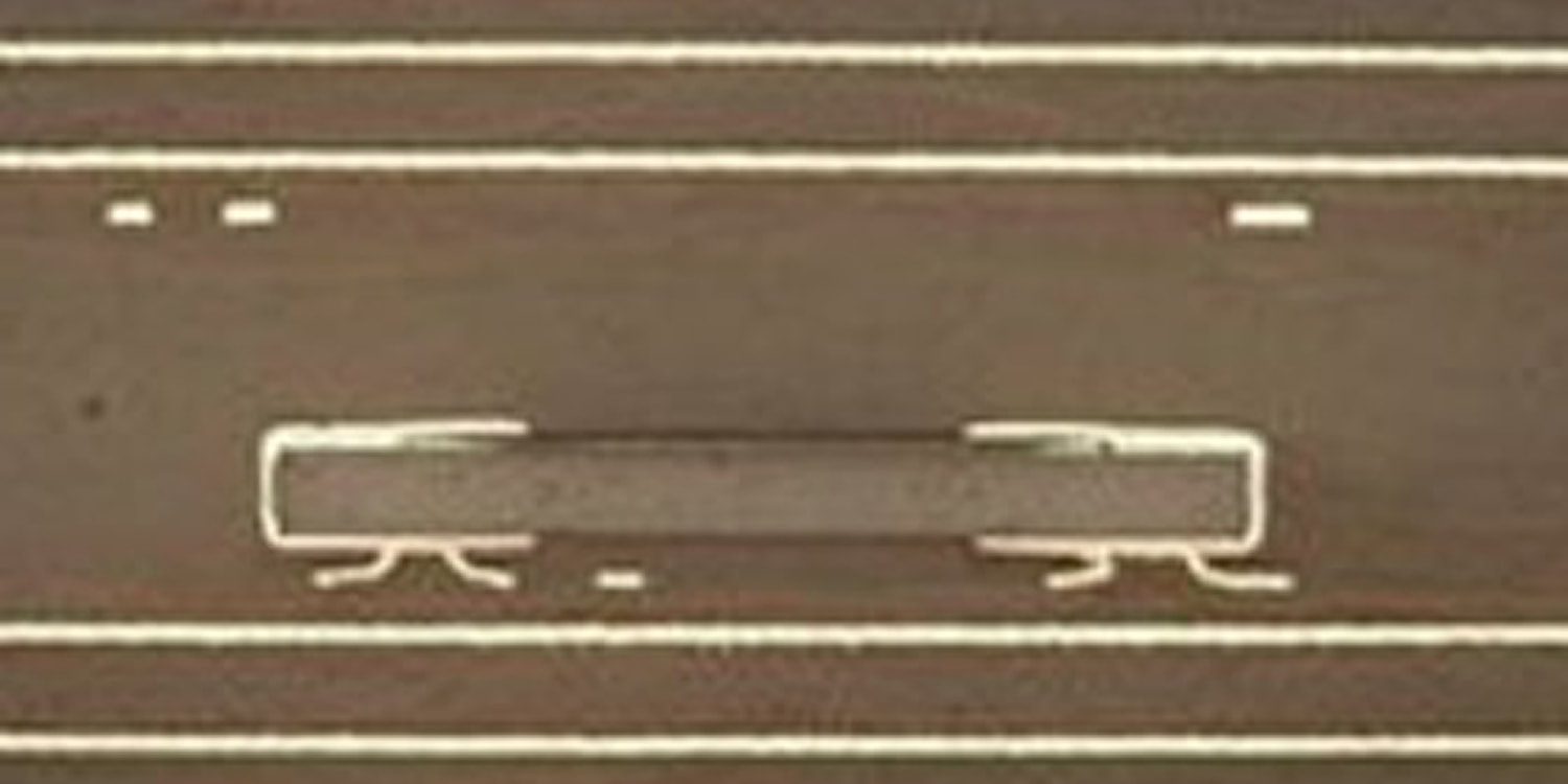
M-VIA Embedded®
We are working on technologies for embedding narrow-pitch electrode bare chips and small passive components to further increase the performance and miniaturization of mobile devices.In addition, as the need for embedding power ICs in automobiles has increased in recent years, we are actively working on technologies for embedding components and simulation technologies that achieve high current and high heat dissipation.
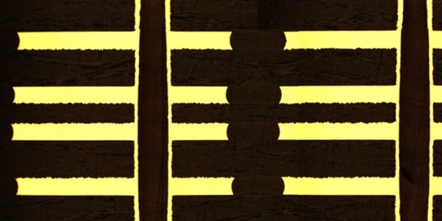
Ultra-Heavy Copper PCBs
We are working on developing ultra-thick copper boards that can carry large currents by increasing the copper thickness of the wiring layer and creating a multi-layer structure.We are working on increasing the thickness of the wiring layer and integral molding using the same resin, and are developing board formation technology that can handle large currents and is highly reliable.
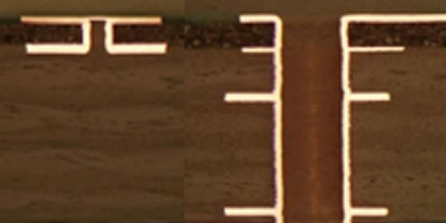
High-frequency hybrid substrate
By creating a hybrid structure using a variety of high-frequency materials (PTFE, LCP, PPE, Low-k Epoxy) and general materials (FR-4), we are able to integrate high-frequency circuits and control circuits to make thinner and smaller boards.We are also working on forming microvias and multi-layering high-frequency materials for higher density wiring.We also conduct in-house evaluations of the material properties and transmission characteristics of new high-frequency materials.
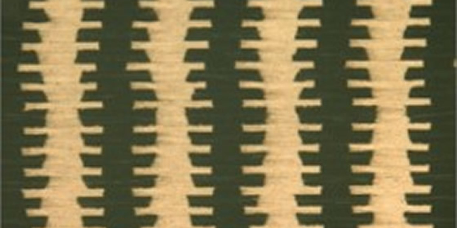
0.3mm Patch CSP Mounting Substrate (M-VIA Any™)
As mobile devices such as smartphones become smaller, lighter, and more multifunctional, 0.35mm pitch CSPs and 0.3mm pitch CSPs are expected to become mainstream in the future. We are working to develop full-layer build-up structures, smaller laser via diameters, smaller via lands, and narrow-pitch circuit formation technologies to accommodate these wiring needs.
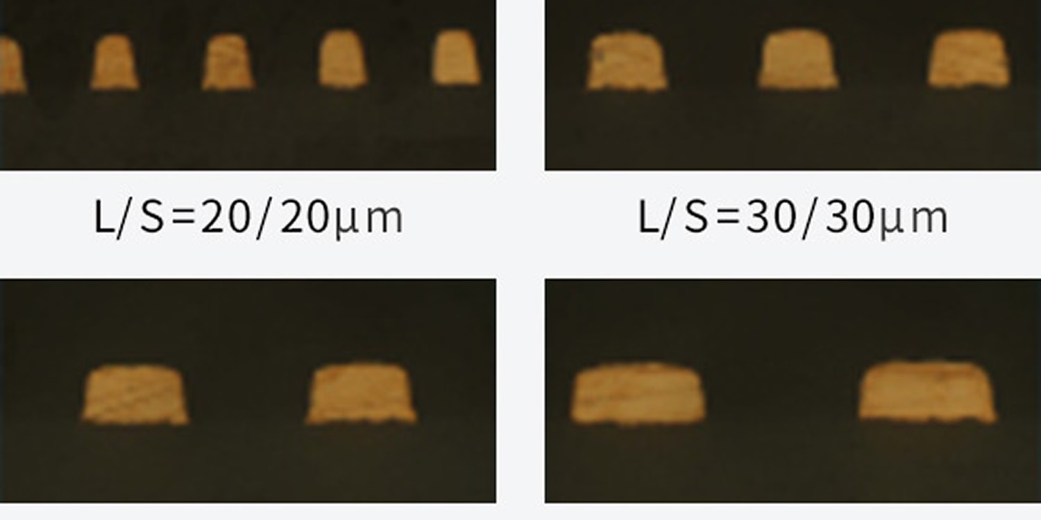
Semi-additive HDI PCBs
To achieve even finer pitch and higher pin count CSPs, it is necessary to increase the number of wires between CSP electrodes from the current 1 to 2 or more, thereby increasing wiring capacity. This will require fine wiring formation technology with L/S = 40/40 μm or less, so we are working on developing a copper foil-based semi-additive method to replace the conventional etching method.
01
PCB Business
Circuit Design
Meiko possesses state-of-the-art CAD systems capable of designing the optimal wiring for a limited space within a short period of time. Fully applying our production know-how straight from the design stage allows us to make the smooth transition to mass production.
Solder Stencils
Meiko provides high-reliability, high-precision, and high-quality solder stencils manufactured in state-of-the-art facilities at our production sites in Japan and other countries. From design to application, our metal masks have a proven record in a wide variety of fields, such as mobile devices, automobiles, and consumer devices. In addition, our integrated production and sales system has enabled us to achieve the shortest delivery times in the industry.
EMS(Electronic Manufacturing Services)
Meiko provides a total solution service to support our customers and help them flexibly adapt to changes in the market. This service integrates the outsourcing of all the processes involved in production, including pattern designing, manufacturing, component procurement, implementation, inspection, and shipment.
02
Electronics businesses
Industrial Equipment
When it comes to PCBs composed of numerous components, it is essential to have inspection technology that verifies the position and size of patterns and holes with micron precision. Meiko uses its PCB manufacturing expertise to provide PCB hole inspection systems and electricity checkers.
Imaging Equipment
Meiko’s imaging division developed and is manufacturing the world’s first multivision video magnifying device (processor) and peripherals, such as matrix switchers and converters. These products are widely used both in Japan and other countries.


