


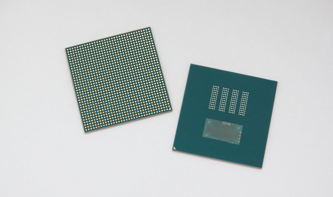
Semiconductor Package Substrate
Semiconductor Package Substrates are minute substrates that act as external connection terminals when mounting semiconductors (IC chips) on printed circuit boards. In order to form minute circuits, Meiko has introduced the MSAP and SAP methods in addition to the Subtrace method, and is also able to produce patterns with L/S=10/10μm.
We have a proven track record in semiconductor memory and CPU applications, and are expanding our manufacturing capacity and conducting research and development both domestically and internationally.
Characteristics of Semiconductor Package Substrates
- Introduction of MSAP and SAP methods for forming ultra-fine circuits
- Also compatible with special ABF materials
- Introduction of coreless method to accommodate thinner designs
Main uses
-

car
-

IoT・AI
-

PC
-
Communication Module
Contact About the productInquiry
In addition to major corporate clients, we also serve universities, research institutes,
We also accept consultations from venture companies.
We also accept one-off orders from design companies and parts trading companies,
Please feel free to contact us for technical advice.

