


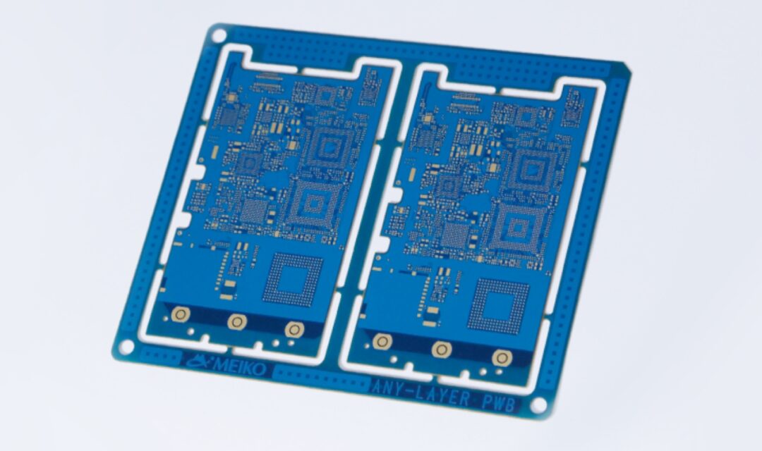
Any Layer PCBs
This is a board with free connection on all layers that combines laser technology, which allows for ultra-fine processing, and fill plating technology. With a high degree of design freedom and the ability to achieve high density, it is an ideal board for meeting the needs of smaller, thinner high-performance devices such as smartphones. Meiko is currently developing the MSAP method for even finer wiring.
High-density substrate
General-purpose PCBs
01
Characteristics of any-layer boards
- High density and thinness achieved through full-layer laser via connections
- Compatible with 0.4mm pitch CSP
02
Main uses
-

Smartphone
-
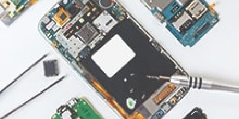
Communication Module
-
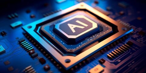
IoT and AI appliances
-

digital camera
Contact About the productInquiry
In addition to major corporate clients, we also serve universities, research institutes,
We also accept consultations from venture companies.
We also accept one-off orders from design companies and parts trading companies,
Please feel free to contact us for technical advice.

